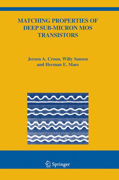
Matching Properties of Deep Sub-Micron MOS Transistors
-
- Hardcover ausgewählt
- Taschenbuch
-
Sprache:Englisch
138,99 €
UVP
160,49 €
inkl. gesetzl. MwSt.,
Beschreibung
Produktdetails
Einband
Gebundene Ausgabe
Erscheinungsdatum
24.03.2005
Abbildungen
XII, 206 p.
Verlag
Springer UsSeitenzahl
206
Maße (L/B/H)
25/16,5/1,7 cm
Gewicht
490 g
Auflage
2005 edition
Sprache
Englisch
ISBN
978-0-387-24314-6
Matching Properties of Deep Sub-Micron MOS Transistors
examines this interesting phenomenon. Microscopic fluctuations cause stochastic parameter fluctuations that affect the accuracy of the MOSFET. For analog circuits this determines the trade-off between speed, power, accuracy and yield. Furthermore, due to the down-scaling of device dimensions, transistor mismatch has an increasing impact on digital circuits. The matching properties of MOSFETs are studied at several levels of abstraction:
A simple and physics-based model is presented that accurately describes the mismatch in the drain current. The model is illustrated by dimensioning the unit current cell of a current-steering D/A converter.
The most commonly used methods to extract the matching properties of a technology are bench-marked with respect to model accuracy, measurement accuracy and speed, and physical contents of the extracted parameters.
The physical origins of microscopic fluctuations and how they affect MOSFET operation are investigated. This leads to a refinement of the generally applied 1/area law. In addition, the analysis of simple transistor models highlights the physical mechanisms that dominate the fluctuations in the drain current and transconductance.
The impact of process parameters on the matching properties is discussed.
The impact of gate line-edge roughness is investigated, which is considered to be one of the roadblocks to the further down-scaling of the MOS transistor.
Matching Properties of Deep Sub-Micron MOS Transistors
is aimed at device physicists, characterization engineers, technology designers, circuit designers, or anybody else interested in the stochastic properties of the MOSFET.
Ein neues Kapitel für Ihre Bücher
Ein neues Kapitel für Ihre Bücher
Schenken Sie Ihren alten Schätzen ein zweites Leben und erhalten Sie dafür eine Thalia Geschenkkarte.
Noch keine Bewertungen vorhanden
Verfassen Sie die erste Bewertung zu diesem Artikel
Helfen Sie anderen Kundinnen und Kunden durch Ihre Meinung.
Kurze Frage zu unserer Seite
Vielen Dank für Ihr Feedback
Wir nutzen Ihr Feedback, um unsere Produktseiten zu verbessern. Bitte haben Sie Verständnis, dass wir Ihnen keine Rückmeldung geben können. Falls Sie Kontakt mit uns aufnehmen möchten, können Sie sich aber gerne an unseren Kund*innenservice wenden.
zum Kundenservice