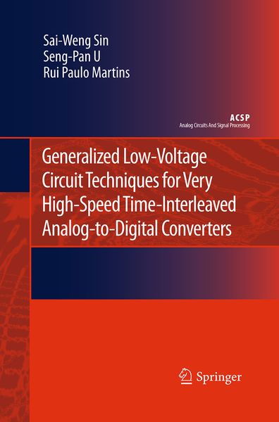
Generalized Low-Voltage Circuit Techniques for Very High-Speed Time-Interleaved Analog-to-Digital Converters
-
- Hardcover
- Taschenbuch ausgewählt
- eBook
-
Sprache:Englisch
93,99 €
UVP
106,99 €
inkl. gesetzl. MwSt.,
Beschreibung
Produktdetails
Einband
Taschenbuch
Erscheinungsdatum
23.08.2016
Abbildungen
XVI, 134 p.
Verlag
Springer NetherlandSeitenzahl
134
Maße (L/B/H)
23,5/15,5/0,9 cm
Gewicht
242 g
Auflage
Softcover reprint of the original 1st ed. 2011
Sprache
Englisch
ISBN
978-94-024-0529-3
Analog-to-Digital Converters (ADCs) play an important role in most modern signal processing and wireless communication systems where extensive signal manipulation is necessary to be performed by complicated digital signal processing (DSP) circuitry. This trend also creates the possibility of fabricating all functional blocks of a system in a single chip (System On Chip - SoC), with great reductions in cost, chip area and power consumption. However, this tendency places an increasing challenge, in terms of speed, resolution, power consumption, and noise performance, in the design of the front-end ADC which is usually the bottleneck of the whole system, especially under the unavoidable low supply-voltage imposed by technology scaling, as well as the requirement of battery operated portable devices.
Generalized Low-Voltage Circuit Techniques for Very High-Speed Time-Interleaved Analog-to-Digital Converters
will present new techniques tailored for low-voltage and high-speed Switched-Capacitor (SC) ADC with various design-specific considerations.
Ein neues Kapitel für Ihre Bücher
Ein neues Kapitel für Ihre Bücher
Schenken Sie Ihren alten Schätzen ein zweites Leben und erhalten Sie dafür eine Thalia Geschenkkarte.
Noch keine Bewertungen vorhanden
Verfassen Sie die erste Bewertung zu diesem Artikel
Helfen Sie anderen Kundinnen und Kunden durch Ihre Meinung.
Kurze Frage zu unserer Seite
Vielen Dank für Ihr Feedback
Wir nutzen Ihr Feedback, um unsere Produktseiten zu verbessern. Bitte haben Sie Verständnis, dass wir Ihnen keine Rückmeldung geben können. Falls Sie Kontakt mit uns aufnehmen möchten, können Sie sich aber gerne an unseren Kund*innenservice wenden.
zum Kundenservice